Скачать с ютуб KiCad 6 STM32 PCB Design Full Tutorial - Phil's Lab #65 в хорошем качестве
KiCad 6 STM32 PCB Design Full Tutorial - Phil's Lab #65
2 года назад
Из-за периодической блокировки нашего сайта РКН сервисами, просим воспользоваться резервным адресом:
Загрузить через ClipSave.ruСкачать бесплатно KiCad 6 STM32 PCB Design Full Tutorial - Phil's Lab #65 в качестве 4к (2к / 1080p)
У нас вы можете посмотреть бесплатно KiCad 6 STM32 PCB Design Full Tutorial - Phil's Lab #65 или скачать в максимальном доступном качестве, которое было загружено на ютуб. Для скачивания выберите вариант из формы ниже:
Загрузить музыку / рингтон KiCad 6 STM32 PCB Design Full Tutorial - Phil's Lab #65 в формате MP3:
Если кнопки скачивания не
загрузились
НАЖМИТЕ ЗДЕСЬ или обновите страницу
Если возникают проблемы со скачиванием, пожалуйста напишите в поддержку по адресу внизу
страницы.
Спасибо за использование сервиса savevideohd.ru
KiCad 6 STM32 PCB Design Full Tutorial - Phil's Lab #65
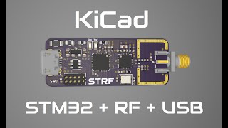
Complete step-by-step PCB design process going through the schematic, layout, and routing of a 'black-pill' STM32-based PCB including USB in the new KiCAD 6. All the way from schematic creation, through to two-layer PCB layout and routing, as well as sending it off for manufacture and assembly via JLCPCB. Mixed-signal hardware design course: https://phils-lab-shop.fedevel.education [SUPPORT] Free trial of Altium Designer: https://www.altium.com/yt/philslab PCBA from $0 (Free Setup, Free Stencil): https://jlcpcb.com/RHS Patreon: / phils94 [LINKS] GitHub: https://github.com/pms67 [TIMESTAMPS] 00:00 Introduction 01:26 What You'll Learn (Schematic) 03:54 STM32 Microcontroller, Decoupling 15:01 STM32 Configuration Pins 21:15 Pin-Out and STM32CubeIDE 26:59 Crystal Circuitry 30:49 USB 33:57 Power Supply and Connectors 42:54 Electrical Rules Check (ERC), Annotation 49:25 Footprint Assignment (Layout) 52:11 PCB Set-Up 57:03 MCU, Decoupling Caps, Crystal Layout 01:03:15 USB and SWD Layout 01:06:37 Changing Footprints, Adding 3D Models 01:09:38 Switch and Connector Placement 01:12:11 Power Supply Layout 01:14:50 Mounting Holes, Board Outline (Routing) 01:19:54 Decoupling, Crystal Routing 01:24:10 Signal Routing 01:27:26 Power Routing 01:32:45 Finishing Touches, Design Rule Check (DRC) 01:35:21 Producing Manufacturing Files (BOM, CPL, Gerber, Drill) 01:39:44 Outro ID: QIBvbJtYjWuHiTG0uCoK
Comments