Скачать с ютуб Introduction to FPGA Part 9 - Phase-Locked Loop (PLL) and Glitches | Digi-Key Electronics в хорошем качестве
Introduction to FPGA Part 9 - Phase-Locked Loop (PLL) and Glitches | Digi-Key Electronics
2 года назад
Из-за периодической блокировки нашего сайта РКН сервисами, просим воспользоваться резервным адресом:
Загрузить через ClipSave.ruСкачать бесплатно Introduction to FPGA Part 9 - Phase-Locked Loop (PLL) and Glitches | Digi-Key Electronics в качестве 4к (2к / 1080p)
У нас вы можете посмотреть бесплатно Introduction to FPGA Part 9 - Phase-Locked Loop (PLL) and Glitches | Digi-Key Electronics или скачать в максимальном доступном качестве, которое было загружено на ютуб. Для скачивания выберите вариант из формы ниже:
Загрузить музыку / рингтон Introduction to FPGA Part 9 - Phase-Locked Loop (PLL) and Glitches | Digi-Key Electronics в формате MP3:
Если кнопки скачивания не
загрузились
НАЖМИТЕ ЗДЕСЬ или обновите страницу
Если возникают проблемы со скачиванием, пожалуйста напишите в поддержку по адресу внизу
страницы.
Спасибо за использование сервиса savevideohd.ru
Introduction to FPGA Part 9 - Phase-Locked Loop (PLL) and Glitches | Digi-Key Electronics
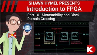
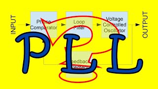
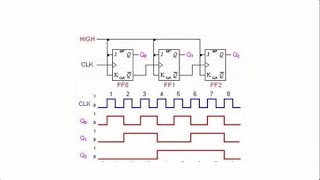
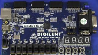
A field-programmable gate array (FPGA) is an integrated circuit (IC) that lets you implement custom digital circuits. You can use an FPGA to create optimized digital logic for things like digital signal processing (DSP), machine learning, and cryptocurrency mining. Because of the FPGA’s flexibility, you can often implement entire processors using its digital logic. You can find FPGAs in consumer electronics, satellites, and in servers used to perform specialized calculations. In this series, we will see how an FPGA works and demonstrate how to create custom digital logic using the Verilog hardware description language (HDL). Previously, we showed how to use block RAM to store data in an FPGA ( • Introduction to FPGA Part 8 - Memory ... ). In this episode, we will see how to use a phase-locked loop (PLL) to increase the clock speed as well as discuss how glitches can occur. The solution to the challenge at the end of the episode can be found here: https://www.digikey.com/en/maker/proj... All code examples and solutions for this series can be found here: https://github.com/ShawnHymel/introdu... A phase-locked loop (PLL) is a digital circuit that produces a repeating pattern (e.g. sinewave, square wave) with a frequency and phase matched to the input reference signal. PLLs have many uses, including demodulation and clock multipliers. The iCE40 has a built-in PLL circuit that can be configured as a clock multiplier. The feedback mechanism contains a clock divider so that the voltage controlled oscillator (VCO) must output a clock that, when divided, matches the reference signal. In the video, we use the icepll tool to calculate the parameters necessary to produce a 120 MHz clock from the 12 MHz reference signal. We then output that faster clock to a pin and measure it with an oscilloscope. We introduce the concept of glitches, which are spurious transitions that may be incorrect data. For example, a simple adder circuit can introduce glitches due to gate delays. The carry bit takes some time to move through a simple ripple-carry adder/counter, and glitches can be seen on the output before the value is registered in flip-flops. We conclude with a challenge: can you think of another way to design a counter that reduces or eliminates glitches? Product Links: https://www.digikey.com/en/products/d... Related Videos: • Cyclone® III FPGA • Power Management: Powering FPGAs • FPGA's: Low-Cost, High Performance Sp... Related Project Links: https://www.digikey.com/en/maker/proj... Related Articles: https://www.digikey.com/en/pdf/r/rene... https://www.digikey.com/en/videos/d/d... Learn more: Maker.io - https://www.digikey.com/en/maker Digi-Key’s Blog – TheCircuit https://www.digikey.com/en/blog Connect with Digi-Key on Facebook / digikey.electronics And follow us on Twitter / digikey
Comments